
3D Scanning in Electronics: When Technological Progress Creates New Engineering Challenges
This is Part 2 of our ongoing series, How 3D Scanning and Reverse Engineering Address Emerging Challenges in Industry and Technology.
Electronics impact nearly every aspect of modern life, governing how people work, entertain, plan, travel, communicate, relax, and manage health. From computer chips to phones, gaming consoles, smart TVs, audio speakers, kitchen appliances, wearables, and more, electronics are ubiquitous, an integrated and, in many cases, indispensable part of our lives. Yet every advancement makes what might be called the Complexity Paradox more likely. That is, as electronics become more powerful, compact and sophisticated, they almost inevitably become more difficult to design, manufacture, maintain and replace.
For example, take the semiconductor industry. Advanced manufacturing and packaging technologies, including 2.5D and 3D integration, chiplets and heterogeneous integration, are enabling manufacturers to meet the demand for greater functionality posed by high-performance computing and AI, while packing greater functionality into increasingly smaller spaces. But do these remarkable advances in technological progress eliminate engineering challenges? No. In many cases, they create new ones.
For electronics manufacturers, those challenges range from keeping aging production equipment operating to managing the increasingly complex physical geometry of advanced packages. Higher power densities—the result of packing more power-processing capabilities into less space—are creating new thermal-management problems, while supply-chain disruptions and rapidly changing technologies are making it more difficult to obtain replacement components and keep products moving into production.
As with other industries, these challenges have something else in common: they increasingly require engineers to know the physical characteristics of components, assemblies and equipment with an unprecedented degree of accuracy.
That's where 3D scanning and reverse engineering can play an important role.
The Challenge: Keeping Obsolete Electronics and Production Equipment Running
Why It's Emerging
Electronic technology changes rapidly; the now-antiquated Flip Video Camera, Sony Discman, and Apple iPod were all once “cutting-edge” technologies. A component, circuit board, production tool or piece of manufacturing equipment that was considered state-of-the-art only a decade or two ago may now be obsolete. Yet the equipment that uses those components may still be perfectly capable of performing its intended function.
This creates a difficult situation for manufacturers. The original supplier may have discontinued a component, gone out of business or simply moved on to newer technology. Original CAD files and engineering drawings for the original parts may be unavailable, and even if documentation exists, it may not accurately represent a component that has been modified or worn through years of service.
Replacing an entire piece of production equipment simply because one component is no longer available can be enormously expensive and will likely also require downtime during setup.
How 3D Scanning Helps
Reverse engineering via scanning provides another option.
By scanning an existing component, engineers can capture its precise physical geometry and obtain the digital information needed to reproduce it. A point cloud (the massive collection of 3D coordinates that define the surface of a part) generated through 3D scanning can be quickly converted into a mesh (with the points of the cloud connected via lines and vertices) and then into a CAD model that can be used for manufacturing or further engineering.
This approach has already been used to address obsolescence in the electronics industry. In one example, a semiconductor manufacturer faced a potential production shutdown because suppliers could no longer provide replacement parts for aging production equipment. After the existing parts were reverse engineered using 3D scanning, the manufacturer was able to reproduce and reinstall them as needed.
In situations like this, 3D scanning doesn't simply reproduce an old part. It can create a detailed digital representation of the part, turning a physical component that has become an engineering dead end into a valuable source of usable digital design information.
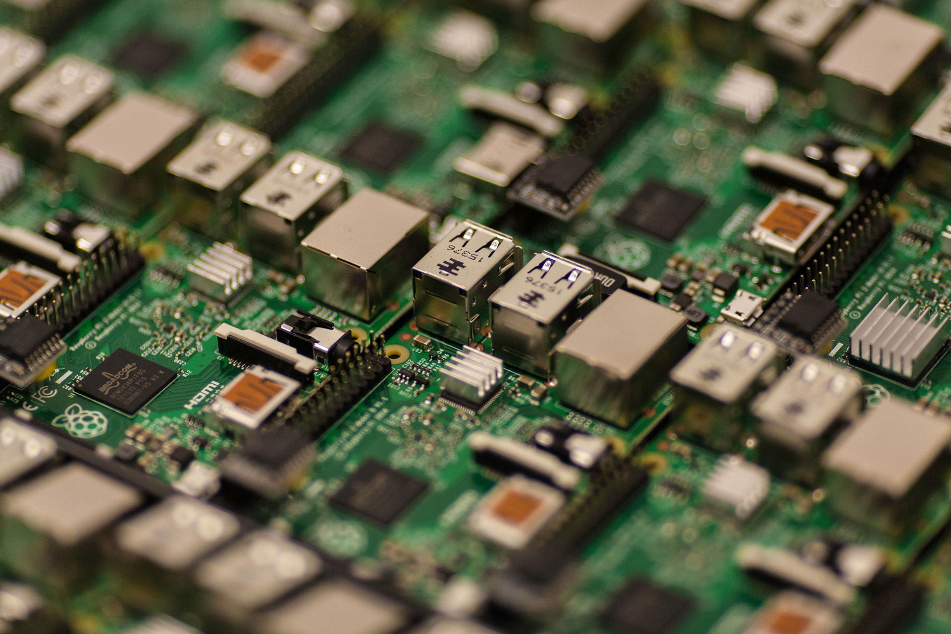
Close-up of a multi-board electronic assembly, where precise 3D scanning can be used to replicate obsolete legacy hardware and legacy components.
The Challenge: Increasing Complexity in Advanced Semiconductor Packaging
Why It's Emerging
As traditional approaches to increasing semiconductor performance encounter physical and economic limits, much of the industry's progress is coming from how chips are packaged and interconnected.
Advanced packaging technologies such as chiplets, 2.5D interposers and 3D stacking allow multiple components to be integrated much more closely than conventional approaches. In 3D architectures, different types of dies can be stacked vertically and interconnected to create highly compact systems with greater functionality and performance.
But packing more components into less space also increases the importance of knowing the precise physical geometry of the components and structures involved.
Alignment, surface characteristics, interfaces, warpage and mechanical relationships between components can all become critical. As packages become more sophisticated, even small dimensional deviations can have consequences for assembly, reliability and performance.
The result is an emerging engineering challenge: how do you accurately characterize increasingly complex physical structures?
How 3D Scanning Helps
3D scanning provides a way to accurately capture the physical geometry of components and assemblies without relying exclusively on existing CAD data, engineering blueprints or conventional contact measurement.
For example, scanning can be used to characterize package-related hardware, fixtures, cooling components, housings, substrates and other larger-scale physical features associated with advanced electronics manufacturing. The resulting digital models can support inspection, comparison with nominal CAD geometry, reverse engineering and design modifications.
The technology is particularly useful when engineers need to understand the as-built condition of a physical object rather than simply the as-designed condition represented by a CAD model. Whenever parts are mass-produced, small errors occur. That’s to be expected; tight manufacturing tolerances, coupled with physical factors such as tool wear, temperature changes and material variations, will always cause slight deviations from the ideal design. But by comparing the 3D scan of a real, physical part against the nominal CAD geometry (i.e., the computer blueprint of the “perfect” part), manufacturers can see exactly where the real part is slightly warped, too thick, or out of shape.
As advanced electronics become increasingly dependent on precise physical relationships, that distinction becomes more important.
The Challenge: Managing Heat in High-Power Electronics
Why It's Emerging
More powerful electronics generally generate more heat—and today’s increasingly compact designs make that heat more difficult to remove.
This is becoming particularly significant as AI, high-performance computing and other demanding applications drive greater power densities. Three-dimensional integration can make the problem even more difficult because vertically stacked components can create localized hotspots and restrict the pathways available for heat to escape. Thermal management challenges such as nonuniform power densities, thermal expansion mismatches and limited heat-dissipation pathways pose significant challenges for 3D heterogeneous electronics.
Cooling systems themselves are also becoming more sophisticated. Advanced approaches can involve thermal-management features such as heat spreaders, specialized thermal interfaces and even microfluidic cooling structures integrated into electronic packages.
In other words, the electronics industry is facing a structural bottleneck problem: how do you move heat through increasingly complex three-dimensional layouts?
How 3D Scanning Helps
While 3D scanning doesn't measure temperature or replace thermal analysis, it can provide highly accurate information about the physical geometry—essential information that thermal engineers need.
Accurate digital models of heat sinks, cooling channels, housings, interfaces and other components can help engineers understand how physical dimensions and relationships correspond to the intended design. Scanning can also be used to inspect manufactured components, identify deviations from CAD geometry and document existing hardware for modification or redesign.
For legacy equipment, scanning can provide another valuable capability: capturing the geometry of an existing cooling component when original design information is unavailable.
As electronics continue to become more powerful and compact, the physical design of their cooling systems is likely to become just as important as the electronic components themselves.
The Challenge: Supply-Chain Disruptions and Alternate Sourcing
Why It's Emerging
The semiconductor industry has become increasingly dependent on complex global supply chains involving semiconductor manufacturers, packaging and assembly companies, specialized material suppliers and equipment manufacturers.
The surge in demand for AI-related hardware is putting additional pressure on that system. Production bottlenecks have emerged not only in advanced semiconductor manufacturing but also in advanced packaging and the supply of substrates, materials and other critical components.
For electronics manufacturers, this creates a problem that extends beyond simply finding a new supplier.
A replacement component may be functionally equivalent but physically different. It may have different mounting features, dimensions, interfaces or other characteristics that prevent it from fitting cleanly and functionally into an existing assembly.
This is where physical compatibility can become just as important as electrical compatibility.
How 3D Scanning Helps
3D scanning can help engineers compare existing and replacement components and document the physical characteristics of parts for which complete design information is unavailable.
It can also support the development of replacement components by capturing the geometry of an existing part and converting that information into a CAD model suitable for redesign or manufacturing.
For manufacturers confronting an unexpected supplier change, this can provide a path toward alternate sourcing without requiring engineers to start the design process from scratch. 3D scanning can essentially help turn a supply-chain problem into an engineering problem—one that can potentially be addressed through measurement, modeling and reverse engineering.
Instead of waiting on a disrupted supplier for lost blueprints, 3D scanning allows companies to capture the geometry of a physical part and recreate its digital design files in-house. This shifts the bottleneck from an uncontrollable logistics delay to an engineering task that can be solved internally through measurement and reverse engineering, providing digital design information that can be supplied to an alternate manufacturer.
The Challenge: Rapid Product Development and Shorter Design Cycles
Why It's Emerging
Electronics companies are under constant pressure to introduce new products faster. At the same time, products are becoming more complex, and the physical relationships among components are becoming increasingly important.
The result is a difficult combination: more engineering information is needed, but there is less time available to obtain it.
This “need for speed,” coupled with the necessity of capturing greater volumes of data, is especially challenging when engineers need to incorporate existing physical components into a new design, reproduce an existing product, modify legacy hardware or understand a competitor's or supplier's component for legitimate engineering purposes.
Traditional measurement methods can require considerable time, particularly when components have complex freeform surfaces or numerous features.
How 3D Scanning Helps
3D scanning can be far faster than legacy measurement methods such as calipers and toolmakers' microscopes. It also provides greater data density and faster data capture. It can rapidly capture large amounts of dimensional information from a physical object and convert that information into an accurate digital model.
Rather than measuring individual features one at a time, engineers can capture an object's overall geometry and then extract the measurements needed from the resulting digital data. That data can support CAD modeling, inspection, design modification and reverse engineering.
The advantage isn't simply speed. It is the ability to create a digital representation of the physical object that can be used repeatedly throughout the engineering process.
For electronics manufacturers working under increasingly compressed development schedules, 3D scanning can help shorten the path from physical component to usable engineering data.
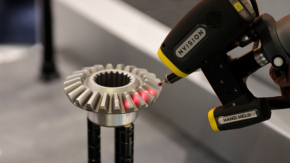
Accelerating the design cycle: NVision’s handheld laser scanner captures the complex 3D geometries of physical components, allowing engineers to rapidly generate digital models for prototyping and development.
Turning New Challenges into New Opportunities
The electronics industry illustrates an important theme of this series: Technological progress doesn't always make engineering problems disappear. Sometimes it simply changes them. New advances often result in new challenges.
Electronics become smaller, creating new dimensional and thermal challenges. Components become obsolete while the equipment that uses them remains in service. Supply chains become more complicated or precarious, creating the need for alternate sources. Product development accelerates, leaving engineers less time to gather the information they need.
In each case, the underlying problem is somewhat different. But they share a common requirement: accurate information about the physical world.
3D scanning can provide that information by capturing the dimensions, geometry and physical characteristics of existing components and assemblies and converting them into usable digital engineering data.
As the electronics industry continues to evolve, that ability is becoming increasingly valuable—not because 3D scanning is a brand-new technology, but because the challenges created by newer technologies are creating new opportunities for its use.
Have an emerging electronics challenge that could benefit from 3D scanning? NVision can help explore the possibilities. Contact us to learn more.
Have an emerging electronics challenge that could benefit from 3D scanning? NVision can help explore the possibilities. Contact us to learn more.
NVision, Inc.
577 Commerce Street, Suite 100
Southlake TX 76092
Tel: (817) 416-8006
sales@nvision3d.com
https://www.nvision3d.com/contact-us